
As semiconductor processes become more miniaturized and complex, the importance of technologies that ensure the durability of equipment components and the stability of processes is also increasing. One of the key technologies for protecting component surfaces under extreme environments—such as plasma exposure—is Thermal Spray Coating.
As the name suggests, thermal spray coating is a technique that melts coating materials using heat and then sprays them at high speed onto component surfaces to form a dense and durable protective layer.
Depending on the type of heat source used, thermal spray coating can be categorized as follows:
- APS (Atmospheric Plasma Spray) — Uses plasma as the heat source
- Arc Spray — Uses an arc discharge between two electrodes as the heat source
- HVOF (High Velocity Oxy-Fuel Spraying) — Uses a high-temperature flame generated by fuel and oxygen combustion
- Flame Spraying — Uses a standard fuel gas and oxygen flame as the heat source
In this article, we will focus on APS coating, exploring its technical definition and the background behind the material transition from APS-Al₂O₃ to APS-Y₂O₃ in semiconductor etching processes.
■ What is APS Coating?
APS (Atmospheric Plasma Spray) is a coating technique that, as the name suggests, involves spraying molten powder particles using plasma generated in an atmospheric environment. In this process, gases such as argon (Ar), hydrogen (H₂), and helium (He) are ionized using electrical energy to create a plasma flame exceeding 10,000°C.
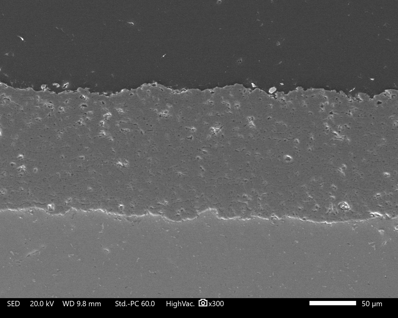
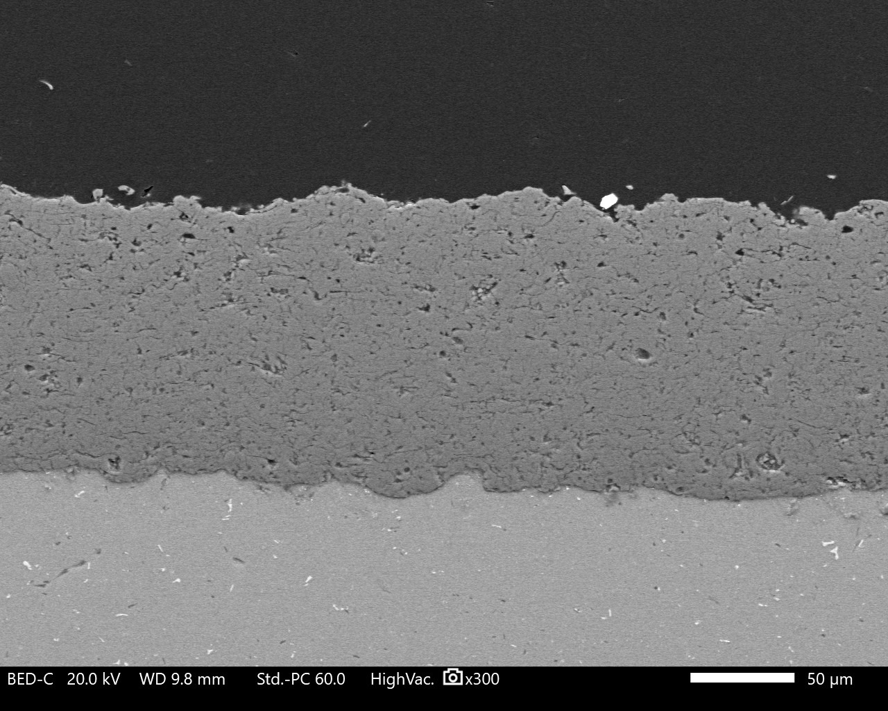
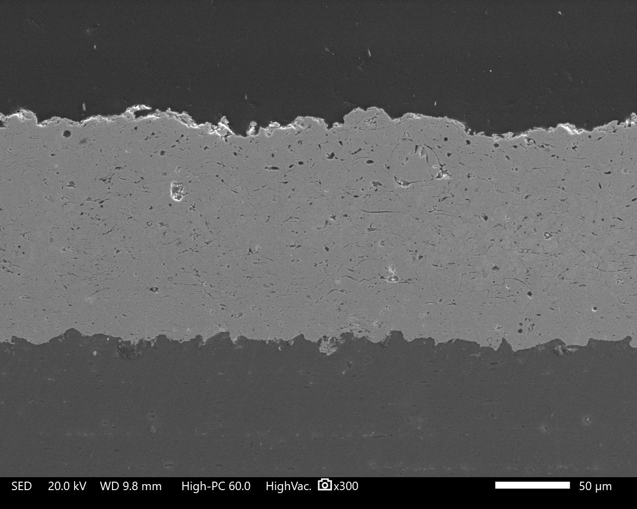
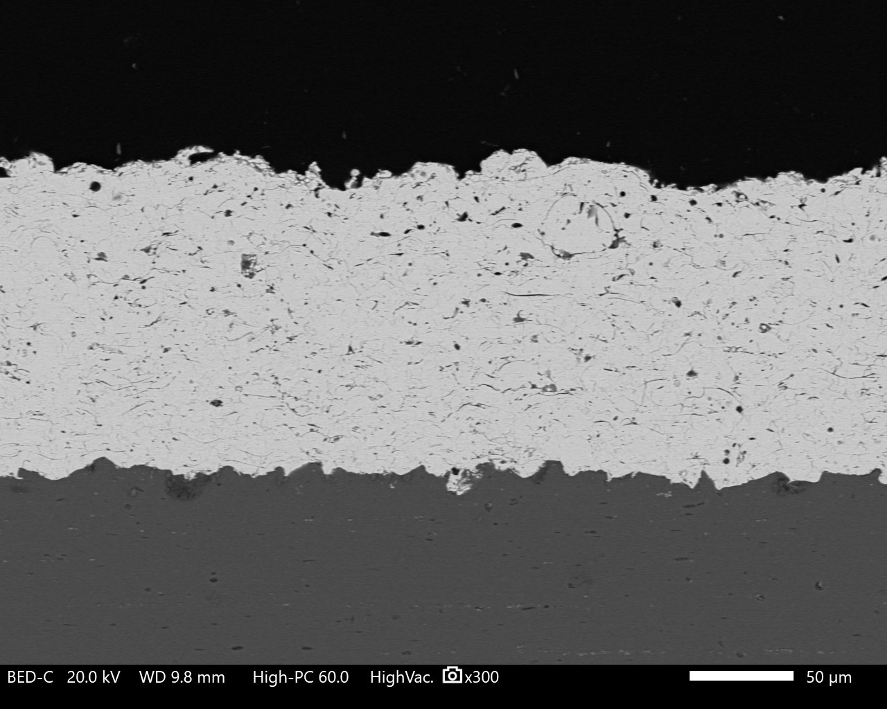
When ceramic powder is injected into this high-temperature plasma, the particles are instantly melted and propelled at speeds of several hundred meters per second, impacting the substrate surface and forming a coating layer. This process is repeated hundreds of times, resulting in multiple stacked layers—each only a few micrometers thick—that ultimately form a dense and robust ceramic coating with a total thickness of approximately 100 to 300 µm.
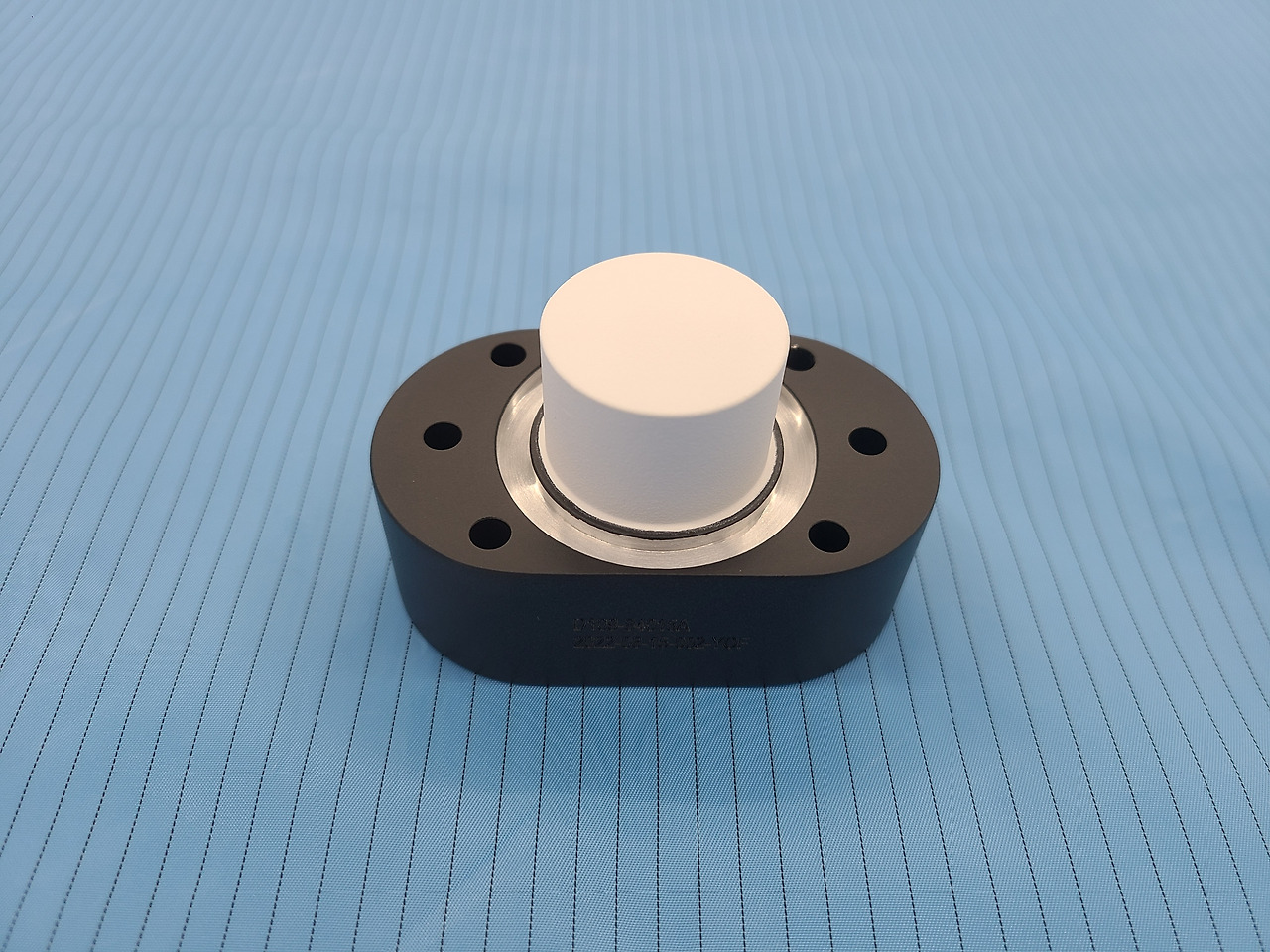
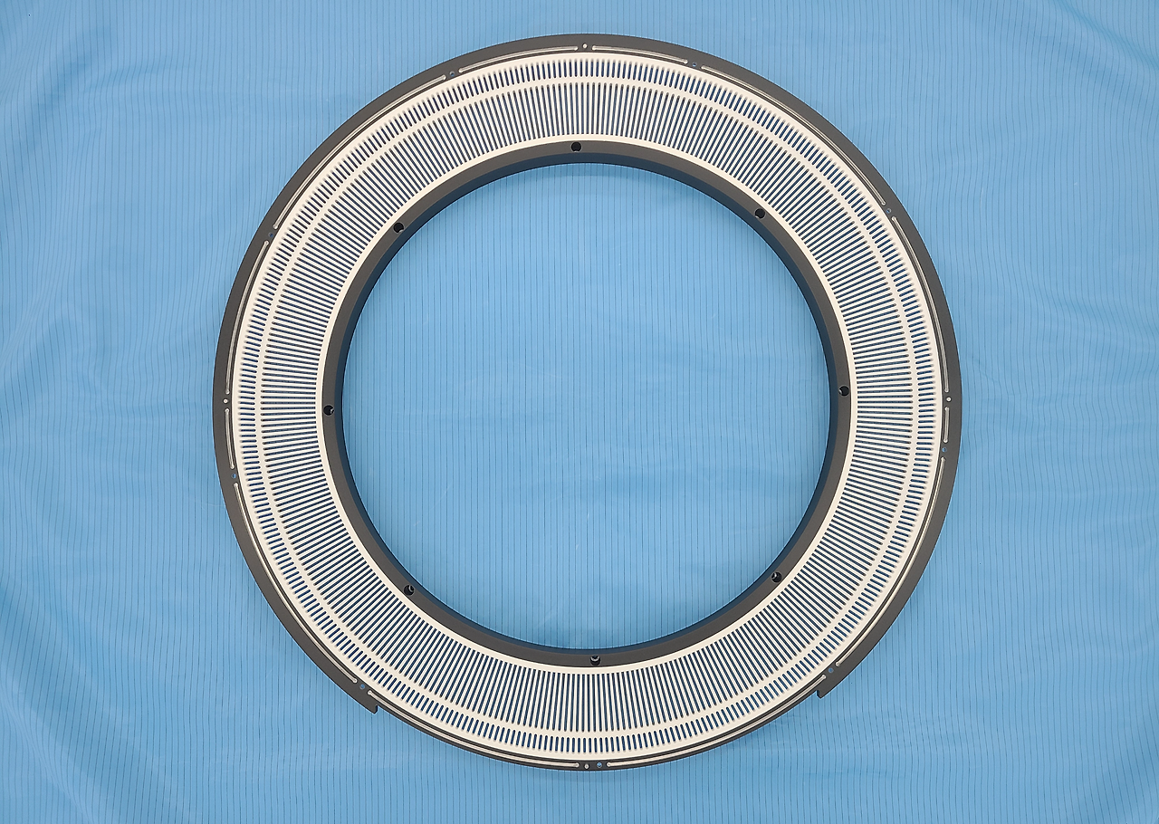
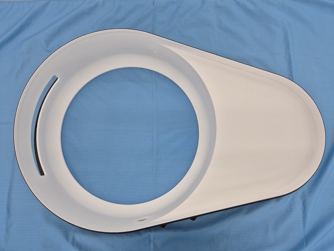
APS coating is especially critical in semiconductor etching (Etch) processes, where the equipment's inner surfaces and key components are continuously exposed to high-temperature and chemically reactive plasma environments. By providing a durable barrier, APS coatings help prevent erosion, extend component lifespan, and ensure stable operation in harsh process conditions.

In semiconductor etching processes, highly reactive plasmas based on fluorine (F⁻), oxygen (O), and chlorine (Cl⁻) can cause severe chemical damage to equipment components. Under such harsh conditions, the “plasma resistance” capability of APS ceramic coatings becomes one of the most critical technological factors determining both equipment durability and process yield.
APS technology utilizes ultra-high-temperature plasma to completely melt ceramic powders, forming an extremely dense and uniform insulating coating layer. This structure ensures that the surface maintains both chemical and physical stability even during prolonged exposure to reactive plasma, without suffering from erosion.
In addition, APS coatings effectively block chemical etching, recombination reactions, and sputtering caused by plasma ions. As a result, they provide long-term protective performance without degradation, even during extended processing cycles. This leads to a range of benefits, including reduced particle generation, shortened seasoning time, and improved process uniformity, ultimately contributing to higher wafer yields and better equipment uptime.
KoMiCo has leveraged these advantages of APS technology to develop next-generation materials such as UC2™, FineCera™, and SF™, which offer enhanced plasma resistance and deliver outstanding protection in even the most advanced semiconductor manufacturing environments.
■ APS-Al₂O₃: Excellent Corrosion Resistance, Wear Resistance, Insulation, and Thermal Stability
Al₂O₃ (alumina) is a ceramic material composed of aluminum and oxygen, known for its outstanding resistance to corrosion and wear, as well as its excellent electrical insulation and thermal stability. These properties make it highly suitable for use in semiconductor etching environments, especially as it allows for the formation of dense and uniform coating layers, even on components with complex geometries.
The key advantages of APS-Al₂O₃ coatings include the following:
| Category | Description |
| Excellent Plasma Corrosion Resistance | Provides chemical stability against F- and Cl-based plasmas, reducing component erosion rates and extending service life. |
| Minimized Particle Generation | High-density, low-porosity coating layer suppresses sputtering, contributing to improved wafer yield. |
| Outstanding Electrical Insulation | Excellent insulating properties prevent leakage current in electrodes, ESCs, and ring components. |
| High Hardness and Wear Resistance | Hardness in the range of 800–1200 HV offers strong resistance to mechanical wear and improves chamber durability. |
| Thermal Stability and Uniform Thickness | Enables the formation of uniform coatings ranging from tens to hundreds of micrometers thick, maintaining structural integrity even under thermal shock. |
| Superior Cost Efficiency | More economical than Y₂O₃ and YF₃ in terms of raw material cost, making it suitable for large-area components and reducing overall maintenance expenses. |
Thanks to these properties, APS-Al₂O₃ coatings have been widely applied to various semiconductor equipment components, making significant contributions to process stability and extended component lifespan.
Al₂O₃ has been widely used since the early days of the semiconductor industry to protect internal chamber components in etching processes, thanks to its excellent performance relative to cost. In addition to its outstanding fundamental properties—such as heat resistance, electrical insulation, and hardness—Al₂O₃ also offers notable plasma corrosion resistance. These characteristics have made it a popular material not only in the semiconductor field but also across other high-reliability industries such as aerospace, aviation, and automotive.
■ APS-Y₂O₃ : High Chemical Stability, Low Erosion Rate, and Excellent Insulation Properties:
As ultra-high-density semiconductor manufacturing processes below the nanometer scale continue to advance rapidly, various technical challenges are emerging in both equipment and material aspects. In response to these industry demands, APS-Y₂O₃ has proven to deliver both superior equipment protection and process stability, thanks to its high chemical stability, low erosion rate, and excellent electrical insulation, even under the most demanding etching conditions.
The advantages of the APS-Y₂O ₃ include.
| Category | Description |
| Maximized Plasma Corrosion Resistance | Exceptional chemical stability against fluorine-based plasma; significantly lower erosion rate compared to Al₂O₃. |
| Particle Suppression | High-density coating structure minimizes sputtering; maintains stable particle emission characteristics even after seasoning. |
| High Melting Point (2,425 °C) | Maintains structural integrity without cracking or delamination under repeated thermal shocks in etching processes. |
| Excellent Electrical Insulation | Ideal for high-voltage components such as ESCs and focus rings due to strong insulating properties. |
| Extended Equipment Lifespan & Reduced Maintenance Costs | Reduced erosion and defects extend replacement intervals, contributing to lower TCO (Total Cost of Ownership). |
APS-Al₂O₃ has long served as the standard protective coating for semiconductor equipment, thanks to its excellent insulation, mechanical strength, and cost-effectiveness. However, as semiconductor processes become increasingly miniaturized and are exposed to higher plasma energy densities and reactivity, the need for materials with superior plasma resistance and stability has grown. In response, Y₂O₃ has emerged as a major APS coating material, effectively meeting the industry's three core demands: durability, yield, and process stability.
Material selection is essential for both equipment protection and process reliability, and it continues to evolve alongside the rapid advancement of semiconductor technology. Positioned at the forefront of this evolution, KoMiCo leverages its extensive experience and technical expertise to lead the development and application of next-generation coating materials, helping customers enhance their process competitiveness.
In the next installment, we will introduce KoMiCo’s premium plasma-resistant APS coatings, including UC2™, FineCera™, and SF™. We’ll explore how these advanced solutions extend equipment lifespan, improve process yield, and ultimately contribute to greater productivity for our customers.
<About KoMiCo>
KoMiCo, established in 1996, was the first company in Korea to commercialize cleaning and coating services for semiconductor equipment components. With global operations spanning the United States, China, Taiwan, and Singapore, KoMiCo has earned quality certifications from some of the world’s leading semiconductor manufacturers, solidifying its position as a Global No.1 in the industry.
Building on its advanced cleaning and coating technologies, KoMiCo continues to enhance its core business while expanding into the development and supply of key OEM components for semiconductor equipment. Moving forward, the company remains committed to improving customers’ productivity and yield, and aims to become a global leader in the semiconductor component cleaning, coating, and manufacturing industry.
'Business' 카테고리의 다른 글
| [코미코 Lab] APS 코팅 소재의 진화 – Al₂O₃와 Y₂O₃ (0) | 2025.05.08 |
|---|---|
| 코미코, 'SEMICON KOREA 2025' 성황리 마무리 (0) | 2025.02.27 |
| [전시회 참가 안내] 2025 SEMICON KOREA 참가 안내 (0) | 2025.01.21 |
| SEDEX 2024 | 코미코, 반도체 대전 참가 (0) | 2024.10.25 |
| [전시회 참가 안내] 코미코 2024 SEDEX 반도체 대전 참가 (1) | 2024.10.21 |